

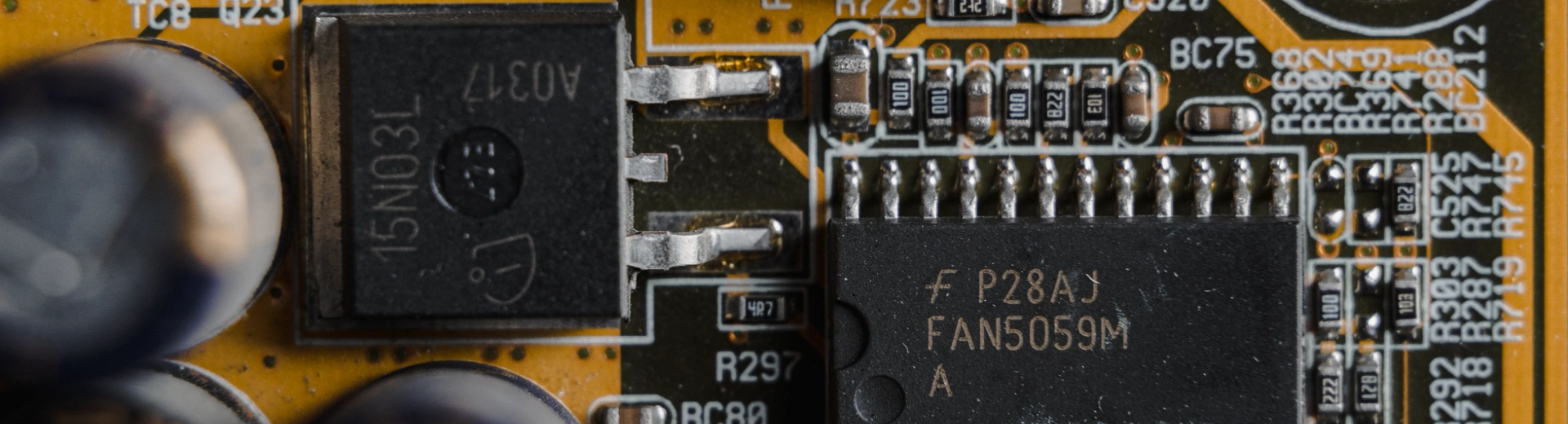
반도체
우리는 시제품 제작, 검증, 장비 통합 및 생산 프로그램을 위한 정밀 제조 부품을 반도체 장비 개발팀에 지원합니다. 우리의 제조 역량은 치수 정확도, 표면 품질, 열 안정성, 청정성, 구조 강성, 배치 간 일관성 등 까다로운 요구사항을 충족하는 데 도움을 줍니다.
Typical Applications:
Powertrain · Chassis · Interior systems · EV components · Testing fixtures

Get Free Quote
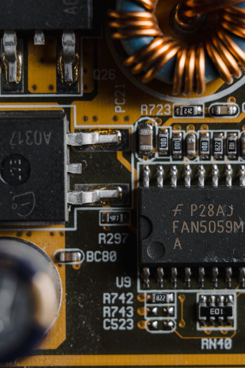
반도체
우리는 시제품 제작, 검증, 장비 통합 및 생산 프로그램을 위한 정밀 제조 부품을 반도체 장비 개발팀에 지원합니다. 우리의 제조 역량은 치수 정확도, 표면 품질, 열 안정성, 청정성, 구조 강성, 배치 간 일관성 등 까다로운 요구사항을 충족하는 데 도움을 줍니다.
Typical Applications:
Powertrain · Chassis · Interior systems · EV components · Testing fixtures
Get Free Quote
반도체 장비를 위한 정밀 제조
반도체 장비 부품은 종종 엄격히 통제된 기계, 열, 진공 및 화학 환경에서 작동합니다. 성공적인 제조는 단순히 부품을 명목 치수로 생산하는 것 이상을 요구하며, 중요한 인터페이스, 표면 조건, 재료 거동, 조립 반복성을 세밀하게 제어해야 합니다
핵심 제조 요구사항

엄격한 치수 및 기하학적 공차

제어된 평탄성과 평행성

안정적인 열 및 구조적 성능

매끄럽고 세척 가능한 표면 상태

진공 및 화학 호환 재료 선택

프로토타입과 생산 배치 전반에 걸쳐 일관된 품질
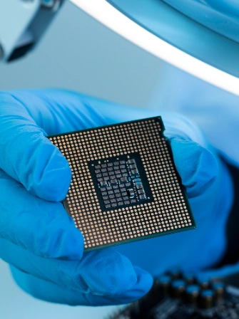

우리가 제조하는 반도체 장비 부품
저희는 웨이퍼 가공 장비, 검사 시스템, 자동화 모듈, 열 관리 조립체 및 반도체 기계 지원 부품을 제조합니다. 저희 서비스는 초기 프로토타입, 기능 테스트 부품, 장비 개발 배치, 생산 준비가 된 부품을 포함합니다.

공정 및 웨이퍼 취급 구성 요소
-
진공 챔버 하우징
-
챔버 뚜껑과 덮개
-
웨이퍼 캐리어 및 트레이
-
웨이퍼 핸들링 암과 엔드 이펙터

장비 구조 및 운동 구성 요소
-
정밀 장비 기지
-
모션 스테이지와 서포트 플레이트
-
선형 운동 괄호
-
장비 프레임 및 구조 패널
열 및 전력 관리 구성 요소
-
냉각판
-
히트 싱크
-
열 장착 판
-
전원 공급 장치 및 컨트롤러 하우징
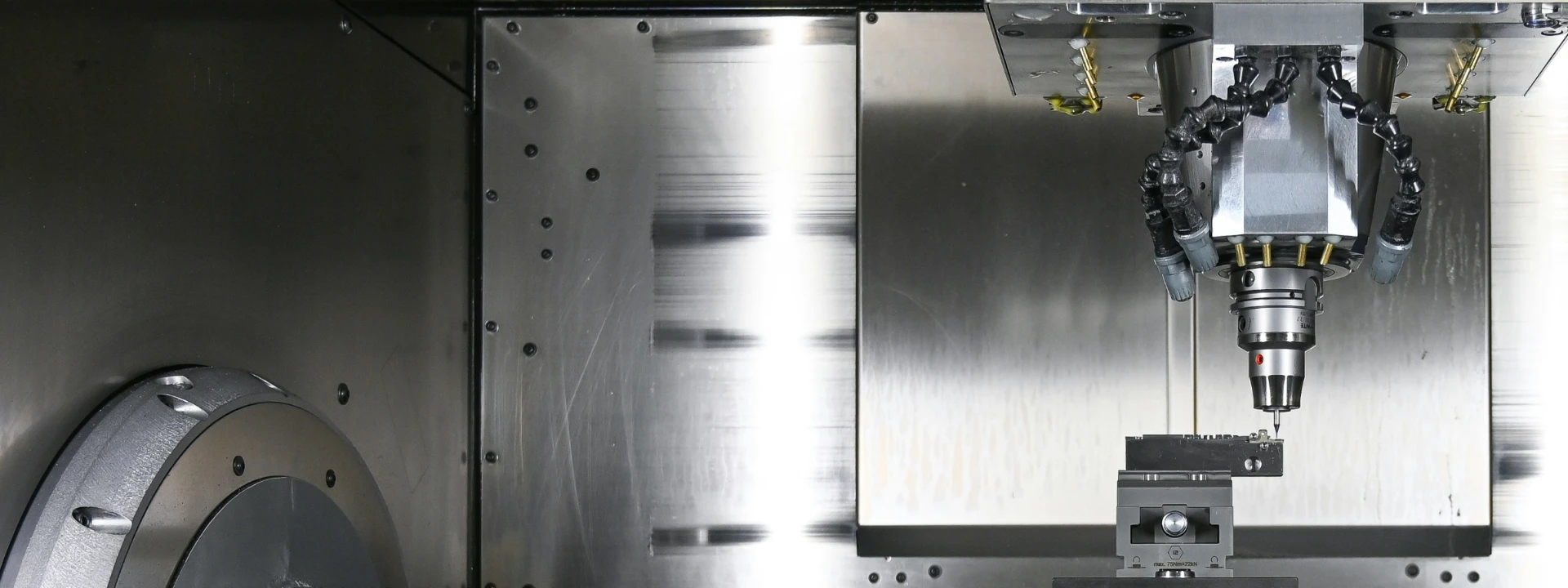
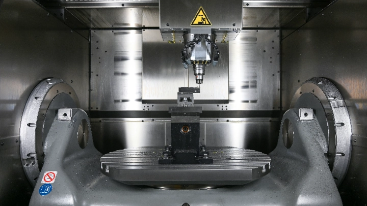

반도체 부품 제조 공정
TOP 프로토타입의 문서화된 능력에는 정밀 가공, 프로토타입 제조, 소량 생산, 3D 프린팅, 판금 성형, 신속 금형, 진공 주조, 후처리 등이 포함됩니다
Request a Quote
반도체 부품의 재료 및 표면 마감
재료 및 마감 선택은 구조 강도, 열 거동, 내식성, 전기 요구사항, 마모 상태, 세척 가능성, 부품의 작동 환경을 기반으로 합니다.

알루미늄 6061 / 6082 / 7075
강도, 가공 가능성, 열전도성, 내식성 등 반도체 장비에서 널리 사용되는 경량 합금입니다.
Typical Parts:
장비 베이스, 챔버 부품, 냉각판, 장착 프레임, 하우징, 정밀 고정구
Explore Materials

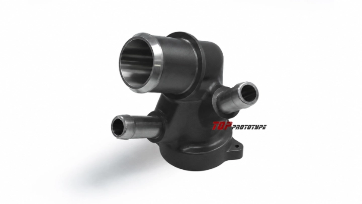
스테인리스 스틸 304 / 316 / 316L
내구성이 뛰어난 금속으로, 우수한 내식성, 기계적 강도, 세척 가능성, 그리고 까다로운 장비 환경에서의 안정성을 제공합니다.
Typical Parts:
챔버 하드웨어, 샤프트, 브래킷, 피팅, 유체 시스템 부품, 정밀 고정구
Explore Materials
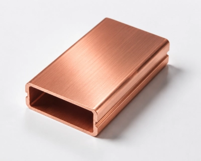
구리 C101 / C110
효율적인 전기 및 열 전달을 위해 고전도성 재료가 선택되었습니다.
Typical Parts:
전도성 판, 전기 접점, 열 스프레더, 버스바, 단자 및 열 부품
Explore Materials
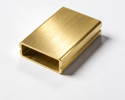
금관
전도성, 내식성, 신뢰할 수 있는 나사산 성능을 결합한 가공 가능한 구리 합금입니다.
Typical Parts:
피팅, 터미널, 나사산 인서트, 커넥터 본체, 계기판, 정밀 하드웨어
Explore Materials
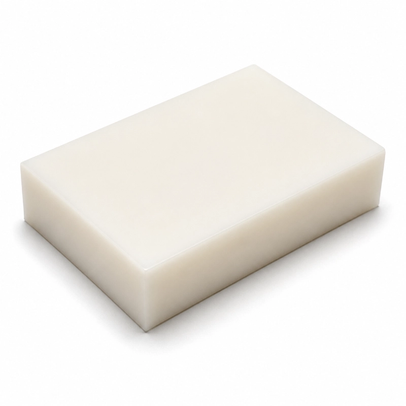
POM
마찰이 적고 마모 저항성이 뛰어나며 신뢰할 수 있는 가공성이 뛰어난 치수 안정성 있는 엔지니어링 플라스틱입니다.
Typical Parts:
가이드, 롤러, 스페이서, 절연 지지대, 위치 조절 부품, 내부 메커니즘
Explore Materials
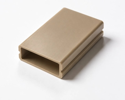
피크 / PPS / PEI
내열성, 화학적 안정성, 전기 절연, 치수 정확도를 제공하는 고성능 공학용 플라스틱입니다.
Typical Parts:
웨이퍼 취급 부품, 절연체, 센서 마운트, 정밀 고정구, 고온 장비 부품
Explore Materials
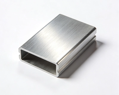
하드 아노다이징
Hard anodizing creates a durable oxide layer on aluminum components, improving surface hardness, corrosion resistance, wear performance, and electrical insulation. It is commonly considered for fixtures, equipment plates, handling components, and high-contact mechanical surfaces.
View Surface Treatment
패시베이션
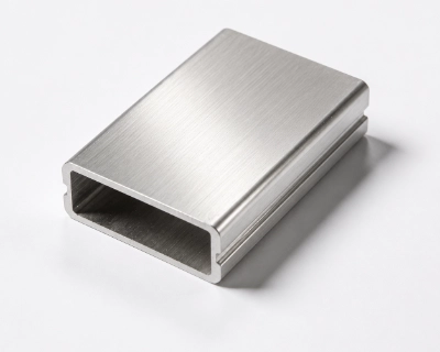
Passivation removes surface contaminants and strengthens the natural protective layer of stainless steel. It is commonly used for precision hardware, shafts, fittings, brackets, chamber-related components, and cleanable equipment parts.
View Surface Treatment
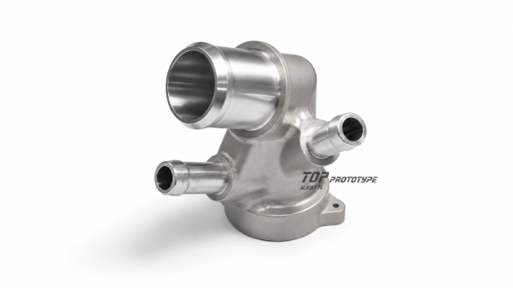
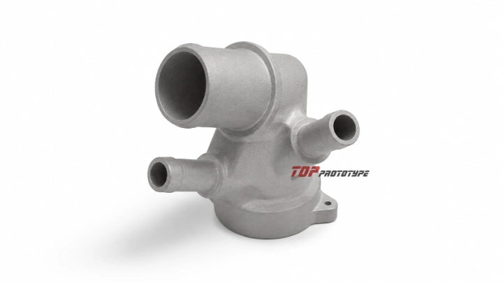
비드 블라스팅
Bead blasting produces a uniform matte appearance and reduces visible machining marks. It is often applied before anodizing or other treatments to improve surface consistency on aluminum and stainless-steel components.
View Surface Treatment
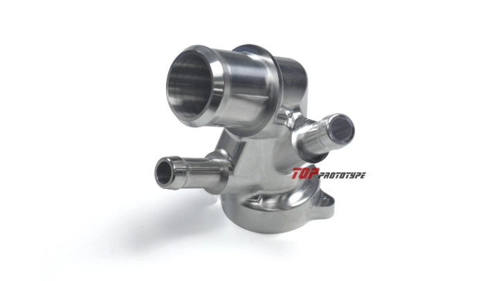
정밀 연마
Polishing reduces surface irregularities and improves smoothness, appearance, and cleanability. It can be applied to contact surfaces, chamber-related parts, fixtures, covers, and components requiring controlled surface conditions.
View Surface Treatment
반도체 FAQ
-
What semiconductor components can you manufacture?

-
We manufacture vacuum chamber components, wafer carriers, handling arms, equipment bases, motion brackets, cooling plates, heat sinks, sensor mounts, optical mounts, housings, fixtures, and automation components.
-
Do you manufacture semiconductor chips or wafers?
-
No. Our capabilities focus on precision mechanical components used in semiconductor manufacturing, inspection, automation, thermal-management, and supporting equipment.
-
Which manufacturing processes are available?
-
Available processes include CNC machining, five-axis CNC machining, CNC turning, precision grinding, sheet metal fabrication, 3D printing, rapid prototyping, and low-volume production.
-
Can you manufacture semiconductor equipment prototypes?
-
Yes. We support prototype components for equipment-development testing, fit verification, assembly evaluation, motion testing, and engineering validation.
-
Can you support low-volume production?
-
Yes. We can support prototype quantities, engineering batches, pilot production, bridge production, and repeatable low-volume manufacturing.
프로젝트 문의 시작
귀하의 정보는 기밀로 유지되며 저희 엔지니어링 팀이 직접 검토합니다. 보통 영업일 1일 이내에 실질적인 기술 피드백을 제공합니다.